研究室
Laboratory
研究室紹介
ナノ物理学研究室
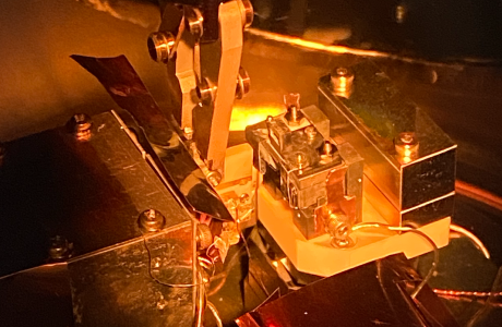
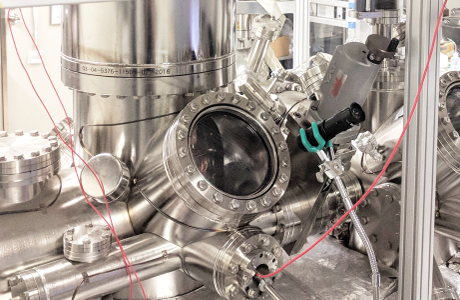
 「ナノ物理学」は、原子と原子の間や、分子と分子の間で起こる量子力学的な現象を観察・解析・制御する新しい物理学の領域です。金沢大学ナノ物理学研究室では、新しい走査型プローブ顕微鏡(Scanning Probe Microscope: SPM)を開発し、その自作装置を使ってナノ物理学を探究しています。
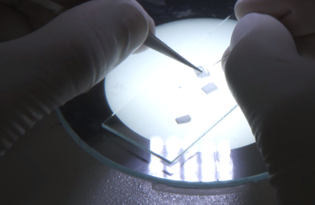
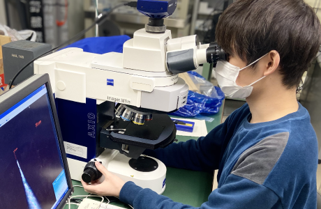
SPMとは、鋭く尖った探針を試料表面に1ナノメータ程度に近づけて、探針と試料間に働く種々の量子力学現象を捉えて、なぞる様にして見る顕微鏡の総称です。私たちは、その中で、トンネル電流を検出する走査型トンネル顕微鏡(Scanning tunneling Microscopy: STM)と、原子間で働く力を検出する原子間力顕微鏡(Atomic Force Microscopy: AFM)及びそれらの複合機を開発しました。今では多くのSPMが市販されていますが、独自開発装置だからこそできる新しい研究に挑戦しています。ナノ物理学研究室の学生は、装置開発のために、機械系・電気系の設計や工作もすれば、実験で得られた未知の現象から新しい物理の構築まで、多岐にわたる研究に取り組みます。
いつも研究室はオープンです。興味のある学生は、いつでも見学に来てください。
以下は、4年生が作った研究室紹介です。
以下では、新井先生の研究紹介動画が見られます。
- サイエンスチャンネル ナノテク未知への挑戦(2) 「ナノの世界にせまる顕微鏡」
この中で、3つの顕微鏡が紹介されています。新井先生は2人目です。 - 金沢大学 研究紹介動画 ココカラ Research25「ナノスケールで探る量子の世界」
研究室行事
ナノ物理学研究室の1年
| 4月 | 新4年生を迎え、新歓コンパ |
| 5月 | (4月−5月)大学院生による新4年生への研究紹介 |
| 6月 | 輪読・論文紹介等ゼミ開始 |
| 7月 | (7月−9月)夏のどこかで国際会議 |
| 8月 | 院試 |
| 9月 | 物理学会・応用物理学会等 |
| 10月 | 院試・秋の学会お疲れ会 |
| 11月 | 日本表面真空学会 |
| 12月 | ニュートン祭・忘年会 |
| 1月 | 卒論・修論追い込み |
| 2月 | 卒論・修論発表 |
| 3月 | 物理学会・応用物理学会等 卒業式・追いコン |
メンバー(2024年度)
スタッフ
| 居室 自然科学5号館 | ||||
| 教授 | 新井 豊子 | あらい とよこ | 425号室 | arai [at] staff.kanazawa-u.ac.jp |
| 助教 | 荒木 優希 | あらき ゆき | 429号室 | y-araki [at] staff.kanazawa-u.ac.jp |
学生
| 学年 | 氏名 | ふりがな | 連絡先 |
| D3 | 加藤 貴洋 | かとう たかひろ | snowballoon [at] stu.kanazawa-u.ac.jp |
| D2 | Voni FULITASARI | フォニ フリタサリ | voni.fulitasari [at] stu.kanazawa-u.ac.jp |
| M1 | 岡部 悠大 | おかべ ゆうた | |
| 花 大地 | はな だいち | ||
| B4 | 入倉 陽斗 | いりくら あきと | |
| 河村 輝 | かわむら ひかる | ||
| 細川 龍治 | ほそかわ りゅうじ |
修了生の主な進路
民間企業
キヤノン(株)、エプソン(株) 、ライオン(株) 、オムロン(株) 、TDK (株) 、 (株)島津製作所、イビデン(株) 、 (株)半導体エネルギー研究所、三菱重工業神戸造船所、カイインダストリーズ(株) 、 SCSK (株) 、 (株)ディスコ、 (株)エンプラス、 (株) SCREENホールディングス
石川県内
(株)PFU、 (株)金沢村田製作所、 (株)フェローテックセラミックス、 (株)別川製作所
富山県内
立山科学(株)
福井県内
(株)福井村田製作所
教員
石川県、滋賀県、富山県、岐阜県、都内私立中学校(母校)
公務員
国、金沢市
About Us
NanoPhysics Laboratory
Nanophysics is a research field that aims at discovery of new physical phenomena by observation, analysis and control of quantum mechanical phenomena between individual atoms and molecules in solid states as well as at explorative development of novel technologies using the phenomena. In our nanophysics laboratory, we develop scanning probe microscopes (scanning tunneling microscope (STM) and atomic force microscope (AFM)) with novel features, and explore nanoscale phenomena by observing and analyzing sample surfaces with atomic resolution, while developing novel nanoscale evaluation methods. From a fundamental scientific question of “How do atoms arrange on solid surfaces and react each other?” to applied science of bottom-up nanotechnology to fabricate novel quantum effect devices by assembling atoms and molecules, we challenge to find the answers and to build up the technology in untrodden fields. The figures below show atom-resolved images of sample surfaces observed in our laboratory using our developed microscopes.
videos introducing prof. Arai
- Science Channel “Microscopes for the Nano World” (in Japanese)
- Kanazawa University Research Videos Research25 “Probing the World of Quantum Mechanics at the Nanoscale” (in Japanese)
Member(2024)
Staff
| Office Natural Science and Technology Hall 5 | ||||
| Professor | Toyoko ARAI | Room 425 | arai [at] staff.kanazawa-u.ac.jp | |
| Assistant Professor | Yuki ARAKI | Room 429 | y-araki [at] staff.kanazawa-u.ac.jp |
Student
| D3 | Takahiro KATO | snowballoon [at] stu.kanazawa-u.ac.jp |
| D2 | Voni FULITASARI | voni.fulitasari [at] stu.kanazawa-u.ac.jp |
| M1 | Yuta OKABE | |
| Daichi HANA | ||
| B4 | Akito IRIKURA | |
| Hikaru KAWAMURA | ||
| Ryuji HOSOKAWA |
Major career paths of graduates
Canon, Fukui Murata Manufacturing, IBIDEN, kai industries, Kanazawa Murata Manufacturing, Lion, OMRON, PFU, SCREEN Holdings, SCSK, Seiko Epson, SHIMADZU, TDK, etc…