

研究紹介
Research
研究テーマ
ナノ物理研究室では、周波数変調原子間力顕微鏡(Frequency Modulation Atomic Force Microscopy:FM-AFM)および、走査型トンネル顕微鏡(Scanning Tunneling Microscopy:STM)との複合機を独自開発し、それらを用いて以下の研究テーマに取り組んでいます。FM-AFMは、超高真空中で使われるとき、探針と試料は非接触で、探針と試料間に働く微弱な引力を検出することから、非接触原子間力顕微鏡(non-contact Atomic Force Microscopy:nc-AFM)とも呼ばれます。研究論文では、超高真空中ではnc-AFM、大気中ではFM-AFMとしていますが、このHP中ではFM-AFMと記載します。


")

ナノ力学的分光法の開拓
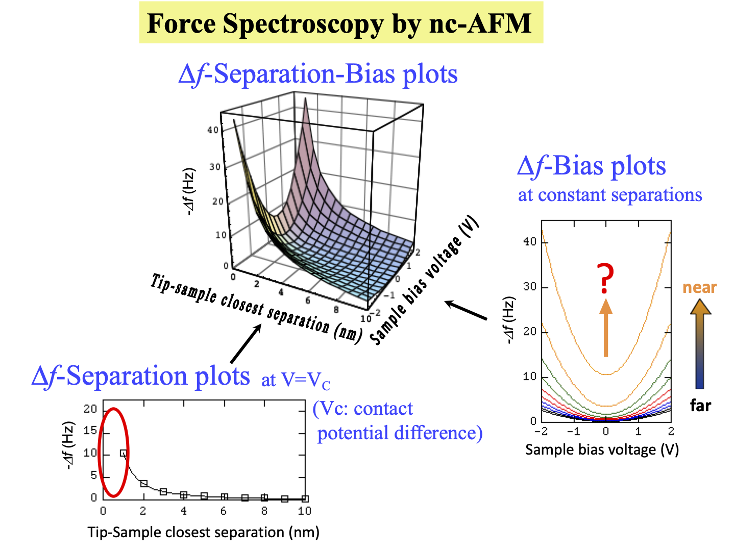
FM-AFMで取得する周波数シフト(∆f)は、探針試料間距離が近づくに従って単調に引力が増加している距離では、マイナスの値をとり、絶対値は単調に大きくなる。探針試料間距離を一定に保って、バイアス電圧(V)を変化させれば、 -∆f は、V2に比例する。長距離力であるvan der Waals力と静電力しか働いていない距離範囲では、下図のように、 -∆fは、距離とバイアス電圧に依存している。では、近距離力(化学結合力)が働く極近距離ではこの3次元プロットの続きはどのようになるだろうか。
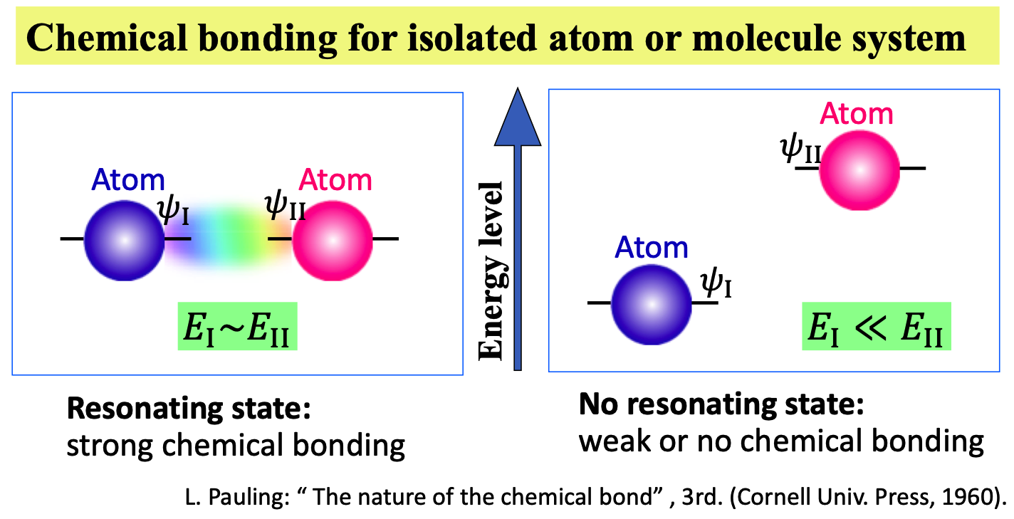
量子力学形成の黎明期、L. Paulingはその著書“The Nature of the Chemical Bond (初版1939)”(日本語訳「化学結合論」)のなかで二原子分子の形成を論じ、最外殻電子のエネルギーがほぼ等しい孤立二原子が接近するとその電子間で量子力学的共鳴(quantum mechanical resonance)が起こり、それが化学結合であるとした。最外殻電子(結合に寄与する電子)のエネルギーがほぼ等しくなければ、化学結合しないことを意味する。
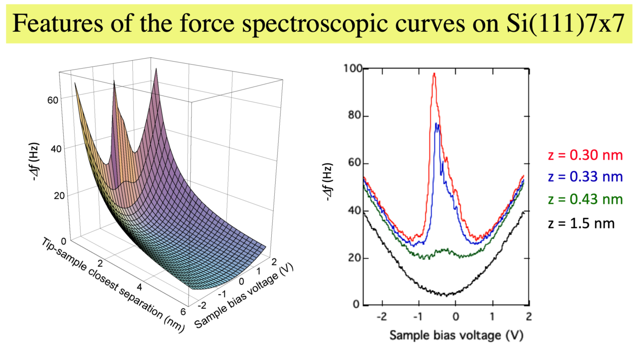
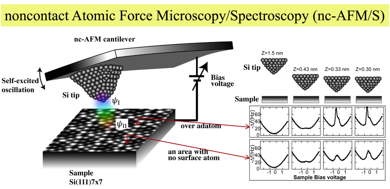
我々は、FM-AFMの探針と試料の間に特定の電圧をかけながら表面を走査すると、探針が試料表面の特定の原子の上に来たとき、探針と試料の間に強い引力が働くことを発見した。これは、探針先端の原子と試料原子のエネルギーが一致したとき、両者に強い相互作用(化学結合力)が生じるためであると推定された。独自開発の超高真空FM-AFM/STM_3 を用いて、探針と試料の間にかけた電圧によって両者の間に働く相互作用の強さがどう変化するかを調べるナノ力学的な分光手法を開拓した(電圧印加非接触原子間力分光法(noncontact Atomic Force Spectroscopy: nc-AFS))。この方法を用いて、探針を試料に接近させ、電圧を少しずつ変化させながら周波数シフト(∆f)を測定したところ、電圧の二乗に比例する静電力とは別に、特定の電圧において強い引力ピークが現れた。すなわち、電圧を制御して、探針原子と試料原子のエネルギーをチューニングして一致させることによって、量子力学的に化学結合が起きることを捉えることができた。
L. Paulingが提唱した「2原子が同じエネルギーを持てば、両者が接近すると量子力学的な共鳴現象で化学結合する」という「孤立系の化学結合論」を、2つの固体表面上の原子間で起こる「凝縮系の表面化学結合論」に拡張できることを実証したことになる。ここで説明した系は探針先端Si原子と、試料表面Si原子間の共有結合力を検出したが、異種原子間でもバイアス電圧によるエネルギーチューニングにより量子力学的共鳴させ、結合するのか、さらに応用して、ナノ構造創製技法に展開できるか研究を続けている。
- T. Arai and M. Tomitori, ” Observation of Electronic States on Si(111)-7×7 through Short-Range Attractive Force with Noncontact Atomic Force Spectroscopy “, Phys. Rev. Lett., 93, 256101 (2004).
ジュール熱散逸計測による表面抵抗の測定
FM-AFMは力センサーの振動振幅が一定になる様に加振しながら、探針試料間相互作用による力センサーの共振周波数の変化(∆f)を捉えます。∆fは、探針試料間相互作用力の距離微分に依存した値を示します。一方で、探針試料間で何らかのエネルギーが散逸すると、力センサーの振動振幅が小さくなり、それを元の一定振幅に戻すために加振のエネルギーを散逸したエネルギー分だけ増加させます。よって探針試料間で散逸したエネルギーをこの加振エネルギーの増加分として計測することができます。また、導電性試料と導電性探針を用いて、探針試料間に電圧を印加すれば、トンネル電流も同時に計測することができます。

探針と試料が導電性で、バイアス電圧(VS)を印加している場合、周波数変化(∆f)は、van der Waals力による周波数変化成分(∆fvdW)、静電力による周波数変化成分(∆fele)、近距離力による周波数変化成分(∆fSR)から成る。
![]() (1)
(1)
また、エネルギー散逸(D)は、力センサー(カンチレバー)の内部抵抗によるエネルギー散逸(Dint)、変位電流が抵抗体を流れることによるジュール発熱によるエネルギー散逸(DJoule)、近距離で起こる非保存の作用によるエネルギー散逸(DSR)に分けられる。
![]() (2)
(2)
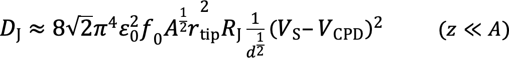
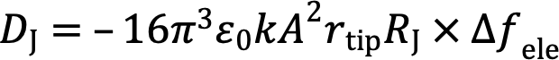
近距離相互作用が働かない距離範囲において、∆feleとDJouleに着目する。探針に対しての資料の接触電位差をVCPDとして、探針試料に連なる抵抗の値をRJとすれば、∆feleとDJouleは以下の様に近似できる。
 (3)
(3)
 (4)
(4)
ここで、f0、A、kは力センサーの共振周波数、振動振幅、バネ定数であり、rtipは探針の先端半径、dは探針試料間最接近距離である。これらの式を見比べると、∆feleとDJouleはどちらも距離dの-1/2乗に比例し、印加電圧![]() の2乗に比例している。2つの式を割ると、
の2乗に比例している。2つの式を割ると、
 (5)
(5)
となり、同時に計測される∆feleとDJouleは距離、印加電圧に関係なく比例していることが分かる。比例係数にはRJを含み、それ以外は、他の計測から知ることができる値である。よって、∆feleとDJouleを同時計測して、その比例係数を求めれば、をRJ求めることができる。
Si(111)7×7再構成表面を試料として、Siカンチレバーを用い、探針試料間距離が数nm程度の位置で印加電圧を掃引して∆feleとDJouleを取得した。
 and the resonant frequency shift due to the electrostatic force interaction (∆<I>f</i><sub>ele</sub>) with respect to the sample bias voltage V<sub>S</sub>.")
この2つのデータから、同じ印加電圧における∆feleを横軸に、DJouleを縦軸に描くと次の図になる。(5)式で見たように確かに∆feleーDJoule図は直線的で、比例関係があることが見てとれる。この直線の傾きから、変位電流が流れた部分の抵抗値が計算できる。

ここで、得られた抵抗とはどこの抵抗だろうか?試料表面に薄膜を形成して抵抗を変化させたり、直列回路の途中に抵抗をいれて計測される結果を比較した。その結果、∆feleとDJouleの値から導いた抵抗値は、探針先端及び、探針先端直径程度の試料領域の試料の表面抵抗を計測していることが分かった。この手法は、非接触で、数十nm程度の空間分解能の平面試料の表面抵抗計測技術として応用が期待される。

散逸エネルギー計測から検知する表面原子変位
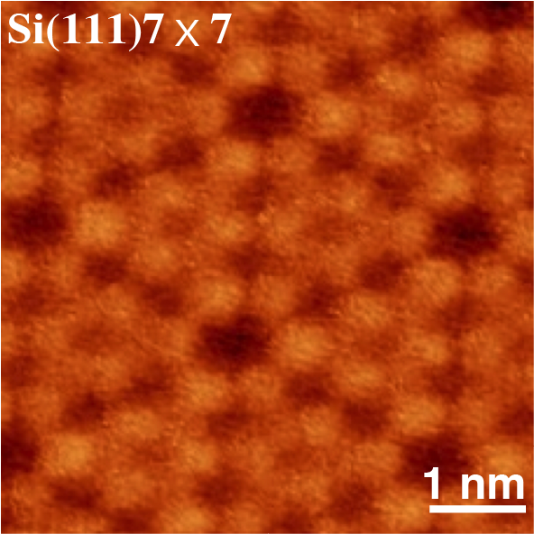
Si(111)-(7×7)再構成表面は、1981年に初めて、走査型トンネル顕微鏡(STM)で原子分解能で表面観察されて以来、多くの研究者がSTMやFM-AFMを用いて原子分解能観に成功している。その原子配列は、室温でも以下に示すDAS(Dimer-Adatom-Stacking fault)構造をしていることが明らかになっている。STMやFM-AFMでは、最表面のAdatomを観察している。
-(7×7) model.")
我々は、Si(111)-(7×7)再構成表面を超高真空FM-AFM/STM_3を用いて、FM-AFM像、トンネル電流像、散逸エネルギー像を同時に原子分解能で観察しました。FM-AFM像は、adatomを凸に描き出し、トンネル電流像では、adatomとrest atomで、電流が多く流れることを示している。しかし、散逸エネルギー像では、表面原子が無い、adatomとrest atom の間のhollow siteで、エネルギーが散逸していることを示した。従来、adatom直上に探針があるとき、adatomを探針が引き上げることで、わずかにエネルギーが散逸する現象を捉えた研究はあった。しかし、ここで計測された散逸エネルギーは、探針の振動1周期あたり0.2 eV/cycleであり、これはadatomの安定サイトのポテンシャルエネルギーと、準安定サイトであるhollow siteのポテンシャルエネルギーとの差に近い値である。我々は、探針及びSi(111)7×7再構成表面に水素を部分的に終端して同様の実験をし、Si探針先端およびadatomとrest atomがダングリングボンドを持つときのみ、そのadatomとrest atomの間のhollow siteで、エネルギー散逸が起こることを突きとめた。そして、探針がhollow site上にあるとき、探針振動の1周期の間で、探針が試料に近づくときにadatomをhollow siteに移動させ、探針が離れるとadatomはまた安定サイトに戻るを繰り返していると考察している。ここで、探針試料間に働く引力は、探針が近づくときよりも離れるときの方が強くなり、このヒステリシスのある力-距離曲線で囲まれた面積分のエネルギーが散逸する。現在、第1原理計算によるシミュレーションで、この現象が再現できるかに取り組んでいる。
-(7×7) in the constant ∆<i>f</i> mode, obtained simultaneously with time-averaged tunneling current <<I>I</I><sub>t</sub>> and energy dissipation images.")

固体表面上のナノメータ厚の極薄水膜(ナノ水膜)
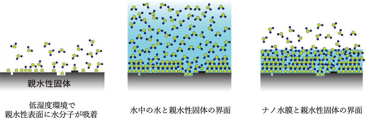
親水性の固体表面には湿度に応じて、水が吸着しています。例えば、低湿度環境で、さらさらした塩(NaCl)の立方体をした結晶の表面にも1分子層の水が吸着しています。この1分子層の水の膜にはNaClを溶かし込む水(液体)としての能力は無く、固体的な性質を示します。一方で、飽和水溶液の中で、溶け残ったNaCl結晶と水との界面では、表面のNa+、Cl-イオンと水和した水分子が水和層を形成します。イオン性結晶以外でも、親水性固体と水との界面には水和層が形成されます。絵では水分子が構造化していて、界面では水分子が動いていないように描かれることがありますが、実際は、水和している水分子の水和の寿命は短く、水バルク中の水分子と常に入れ替わって動いています。
高湿度環境で、吸着水の厚さが水分子10層程度、数ナノメートル程度だったら水/固体界面はどうなるでしょう。ナノ物理学研究室では、数ナノメートル程度の水膜と固体の界面の水和構造は、厚い水膜と固体の界面に比べて硬く結合して固体(氷)に近い擬似固体構造をとり、流動性も低く、液体的な性質と固体的な性質の中間的な性質:準液体性を持つことを明らかにしました。私たちは、固体上に大気中から吸着してできた数ナノメータ厚の水膜をナノ水膜と名付け、研究を続けています。
マイカ上のナノ水膜
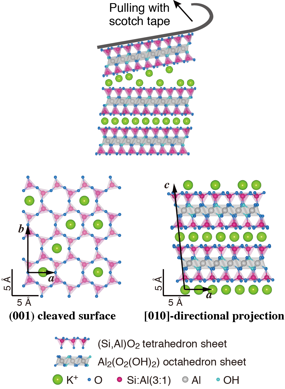
「マイカ(雲母)」は、ケイ酸塩鉱物のグループ名で、組成構造の異なる多くの鉱物がこのグループに属している。マイカの中でも、AFM観察をする人たちの多くが、muscovite (KAl2(Si3Al)O10(OH)2、日本語名:白雲母)を基板として用いていており、AFM像で、マイカ基板と書かれてあったらほとんどの場合モスコバイトのことです。マイカは層状物質で、スコッチテープを表面に張って剥がせば、原子的な平坦面が容易に得られます。そのため生体分子などをAFM観察するための基板として重宝されています。私たちは、モスコバイトを高湿度環境において、モスコバイト上に成長したナノ水膜の界面水和構造を詳しく調べました。25度の実験室の温度で、ナノ水膜も液体ですが、モスコバイトとの界面で、ナノ水膜に「欠陥」があることを見つけました。「欠陥」は固体固有の構造であり、液体に「欠陥」はありません。このことからも、私たちは、ナノ水膜は準液体性であると考えています。
モスコバイトの構造
モスコバイト(KAl2(Si3Al)O10(OH)2)は、SiO2四面体シート間にK+イオンがあり、劈開すると、K+イオンはそれぞれ1/2の確率で両劈開面に残ります。また、SiO2四面体シートのSiの1/4はAlに置き換わっているため、SiO2四面体シートはマイナスの電荷を持ち、K+イオンにより固体全体では、電荷は打ち消されています。
ナノ水膜/モスコバイト界面の水和構造
0%程度の高湿度下にモスコバイト劈開基板を1〜2時間放置しておくと、約2 nmのナノ水膜が形成されます。大気中駆動FM-AFM_4を用いて、ナノ水膜/モスコバイト界面を観察しました。
 images on muscovite surface covered with a nanometer-thick water film")
モスコバイト表面から1 nm程度の距離からモスコバイト表面と同じ周期のFM-AFM(∆f)像がえられ、近づけていくと同じ周期で、異なる像が得られました。一番遠い(右側の)像は第3水和層で、近づけていくと、第2水和層、第1水和層、吸着層を観察しています。像の上半分にはモスコバイトの表面構造モデルを重ねました。水中でのモスコバイトの界面水和層観察でも、上記の像と同様に、第1水和層、第2水和層それぞれの水分子は、モスコバイトの表面の骨格上、表面キャビティ上に配置して観察されています。しかし、水中観察では、第3水和層は観察されていません。これは、ナノ水膜と固体の界面の水和の結合距離が短く、強い結合になっていているためと考えられます。一番左の吸着層の像にはモスコバイト表面のキャビティに残留したK+イオンと考えられる輝点(凸)に緑の○を付けました。それ以外のキャビティには水分子が吸着し、像では弱い輝点になっています。この様に、壁開示に残存したK+イオンを観察できたのも、この研究が初めてです。
ナノ水膜中の欠陥構造
何度も第1水和層、第2水和層を観察していると、水和層の中に欠陥(水分子が構造化していないところ)が観察されました。おそらくこの下のモスコバイト基板に欠陥があるのだと考えられます。水和層中の水分子は同じ層内の水分子同士も水素結合するし、この観察時には、約2nm厚、つまり10分子層程度の水分子が堆積しているので、水膜の中で水分子の流動性が高ければ、基板に欠陥があったとしても水和層に欠陥構造が残ることは無いでしょう。この水分子のモスコバイト基板への界面層の成長は、固体のエピタキシャル薄膜成長様式の1つであるFrank-van der Merwe(FM)成長とよく似ており、ナノ水膜は固体との界面層で擬似固体構造をとっている。ここで、固体膜であれば、AFM像取得時に、表面を破壊すればその痕跡が残るが、この水膜内部の擬似固体層は、下層を画像化した後も、探針を上層位置の高さで画像化すれば、壊れた痕跡はなく、再度、水素結合する柔軟さを持っている。また、固体基板から離れると水分子同士の水素結合が弱くなり液体的になっていくが、すぐに気液界面の律速を受けるため、わずかな流動性しか示さない。これらが、厚い水膜とは異なるナノ水膜の特異性である。

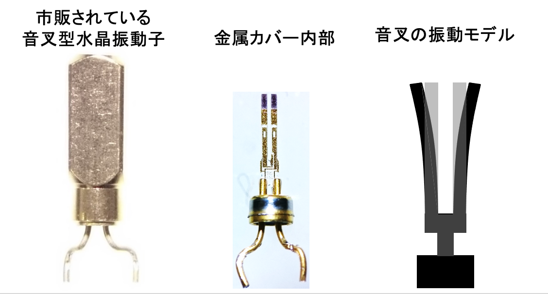
共振再調整力センサーの開発
retuned fork (RTF) force sensor
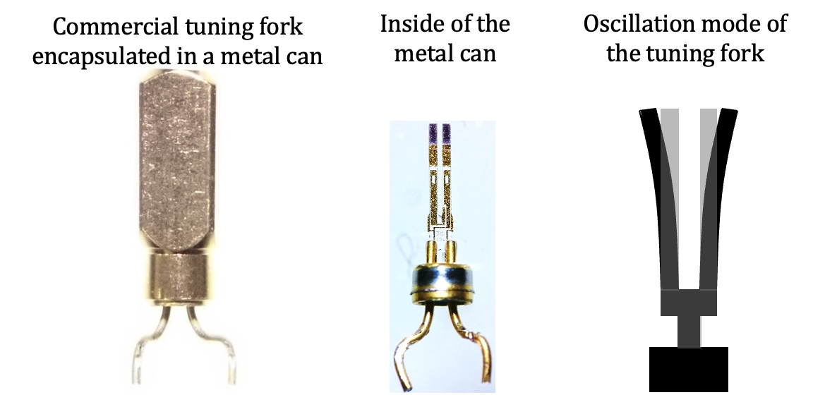
FM-AFMで探針試料間に働く力を検出する力センサーには、一般的に市販のSi製のカンチレバーが用いられている。我々も、大気中駆動FM-AFM_4 では、市販のSi カンチレバーを用いている。しかし、より小振幅で高感度に力を検出するために、腕時計で使用されている音叉型水晶振動子をベースにした共振再調整(RTF)力センサーを開発した。
FM-AFMの高感度化のためには、力センサーの機械的Q値が高いことが求められる。音叉は、2本のプロングが同じ共振周波数で、逆位相で振動することで高いQ値が実現される。しかし、音叉の片方のプロングに探針を形成すると、2本のプロングの共振周波数が異なりQ値が低下してしまう。そこで、探針及び接着剤の重量分、プロングの一部を削り2本のプロングの共振を再調整して高いQ値を持ったRTF力センサーを作った。
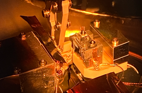
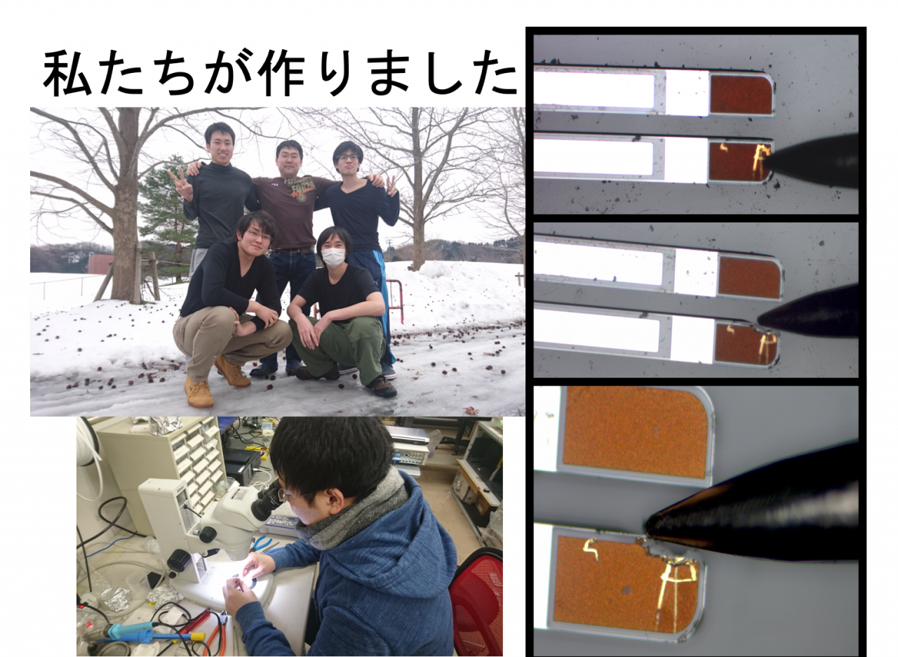
RTFセンサーの作製手順
 音叉型水晶振動子を準備する<br>(b, f) 探針を付ける側のプロングの先端を削る<br>(c, g) 導電性接着剤で探針を削ったプロングに接着する<br>(d, h) 音叉型水晶振動子をセラミック基板に接着し、電気的に配線する")
音叉型水晶振動子のプロングのサイズは 2 x 0.2 x 0.1 mm程度で、削るサイズは0.1 x 0.1 mm程度です。そこに長さ約0.1 mmの探針を接着します。これらの作業は全て実体顕微鏡下での手作業です。
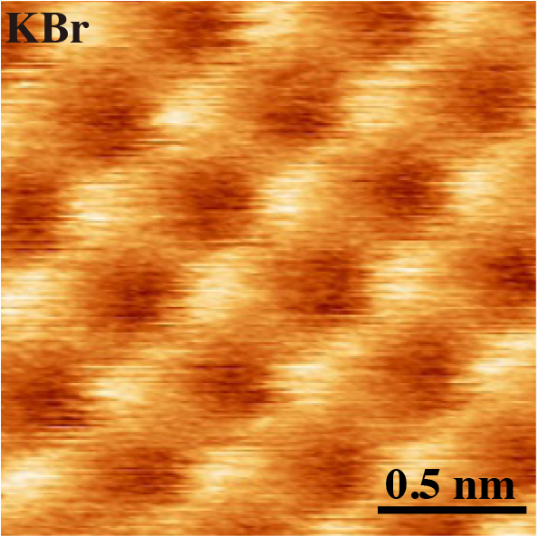
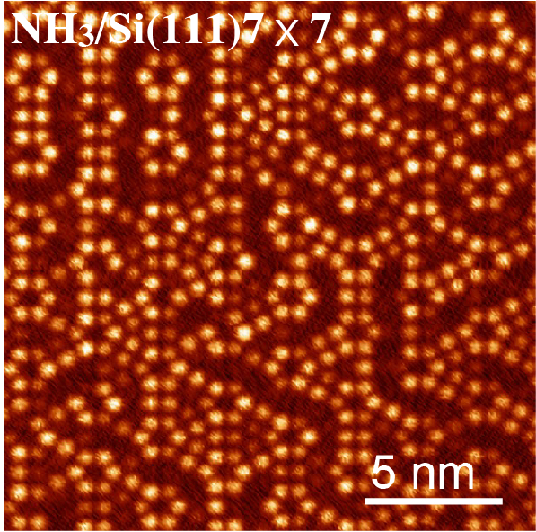
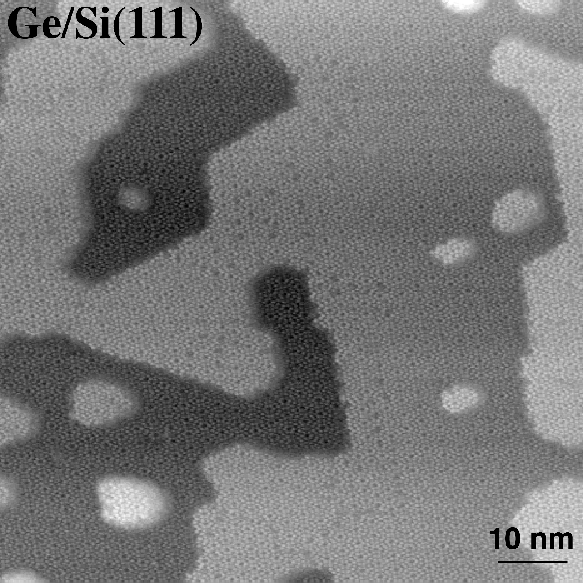
顕微鏡像ギャラリー
開発装置
超高真空極低温FM-AFM/STM_1
UHV LT FM-AFM/STM with retuned fork (RTF) force sensor 1
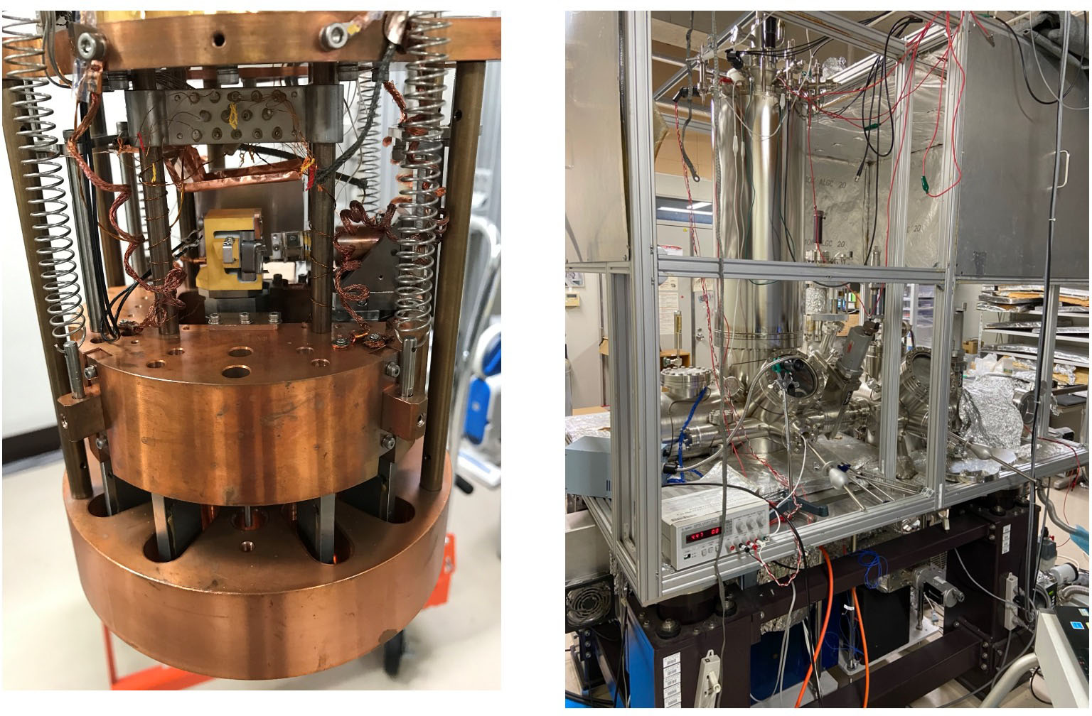
液体ヘリウムタンク型クライオスタットを備えたFM-AFM/STM。FM-AFM用の力センサーには、独自開発の共振再調整(RTF)力センサーを用いている。
自然科学5号館 103-2号室
超高真空FM-AFM/STM_2
UHV FM-AFM/STM with retuned fork (RTF) force sensor 2
超高真空FM-AFM/STM。FM-AFM用の力センサーには、独自開発の共振再調整(RTF)力センサーを用いている。RTF力センサー上に、炎エッチングで先鋭化したタングステン探針を形成する。
自然科学5号館 103-1号室
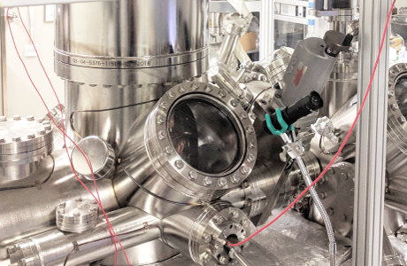
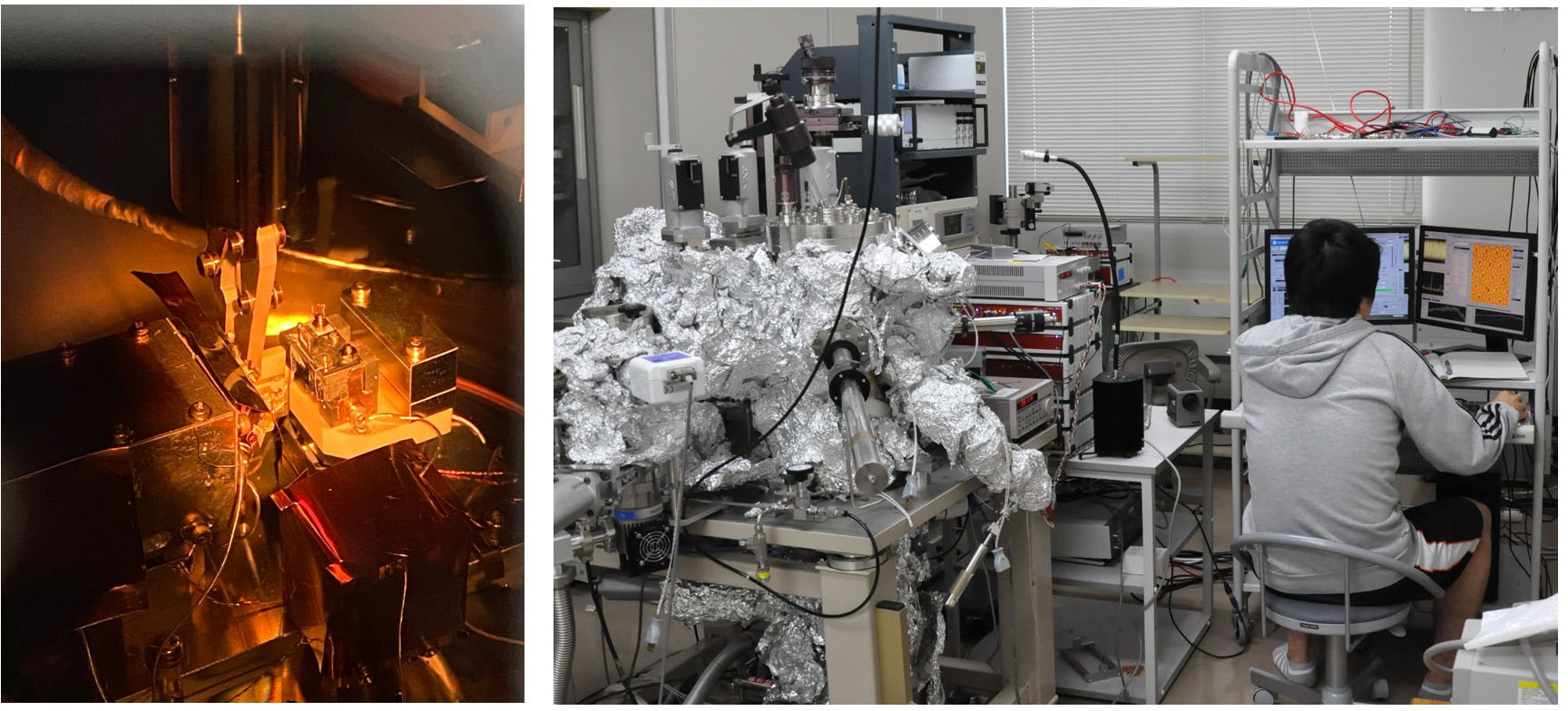
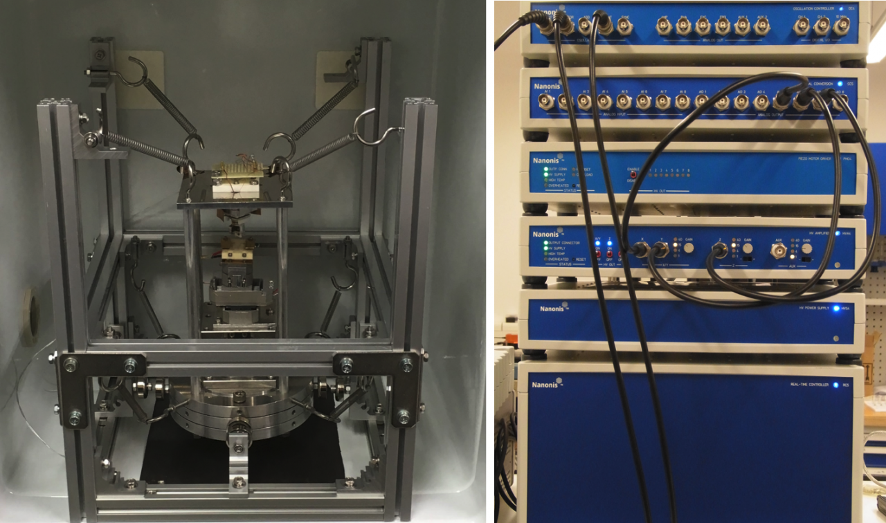
超高真空FM-AFM/STM_3
UHV FM-AFM/STM with piezoresistive Si cantilever
新井教授が最初に立ち上げたFM-AFM/STM。超高真空チャンバー内にはFIM・FEM用蛍光スクリーンがあり、探針のFIM・FEM像観察もできる。
共同研究先の北陸先端科学技術大学院大学に置かれている。
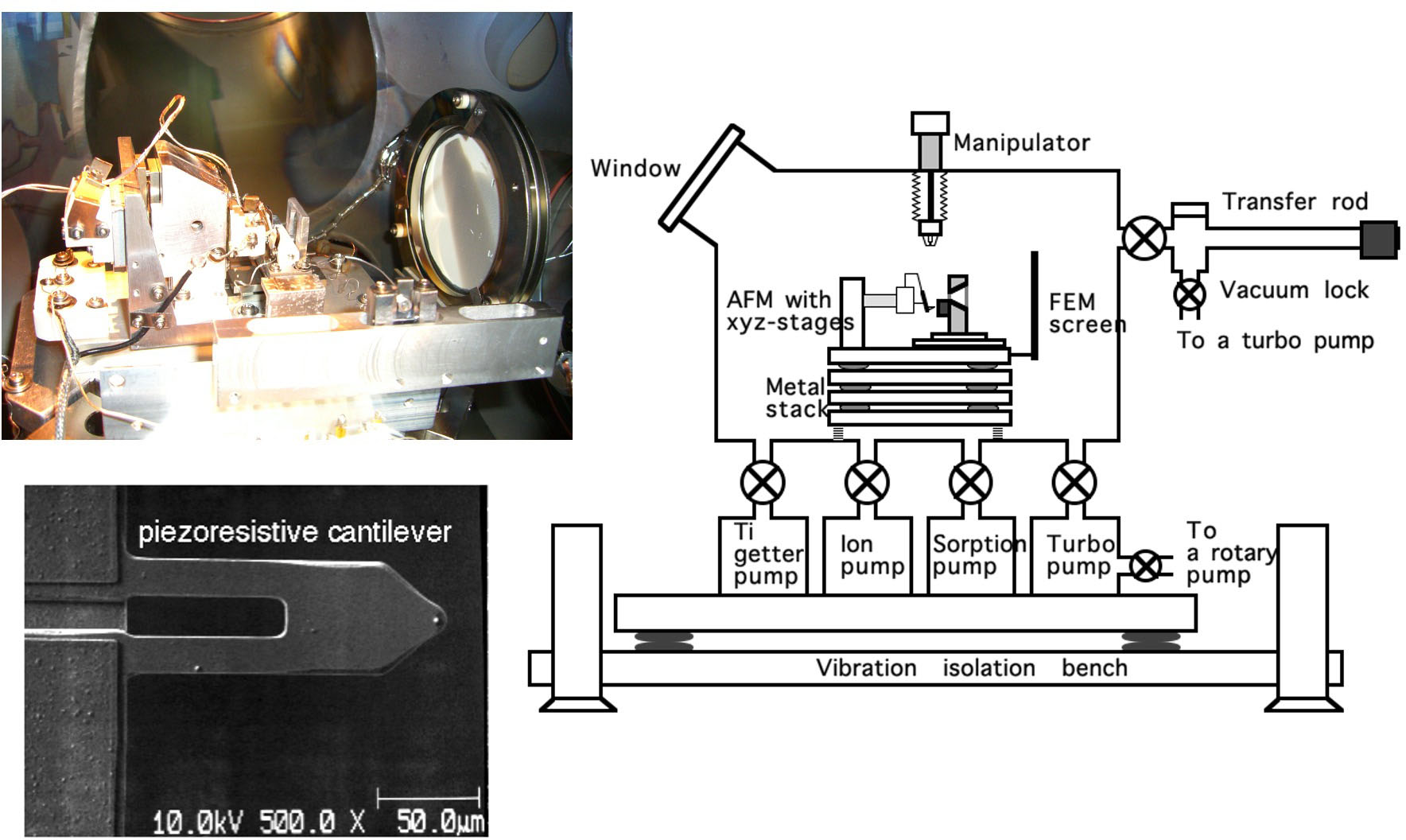
大気中駆動FM-AFM_4
ambient FM-AFM 4
本装置は、科学技術振興機構 先端計測分析技術・機器開発事業の支援を受け、島津製作所製SPM-9600をベースとして構築した大気中駆動FM-AFMです。
自然科学5号館 410-411号室
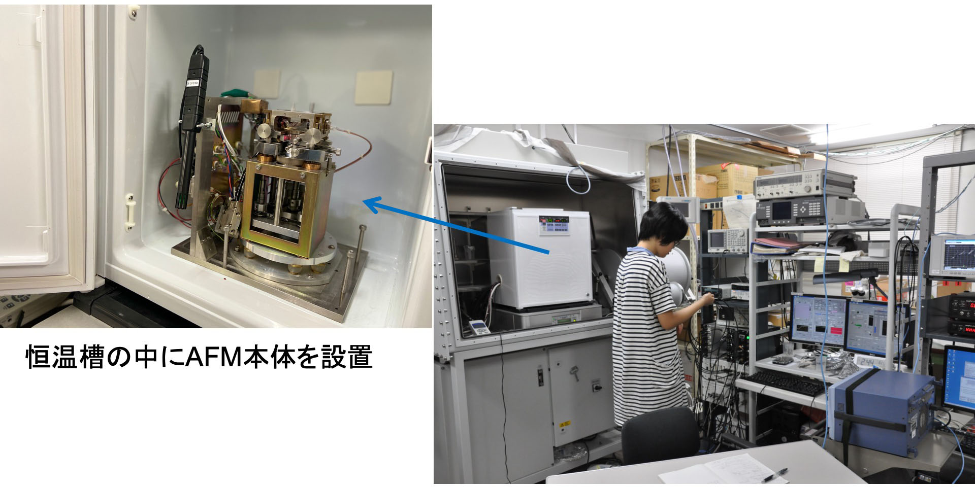
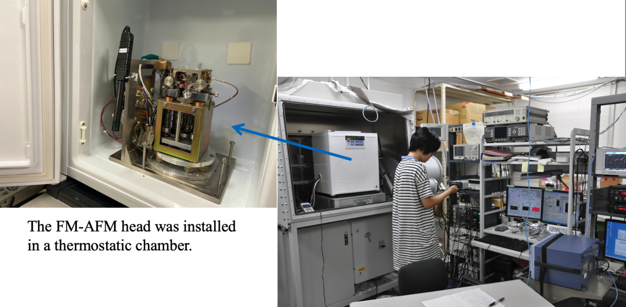
大気中駆動FM-AFM_5
ambient FM-AFM 5
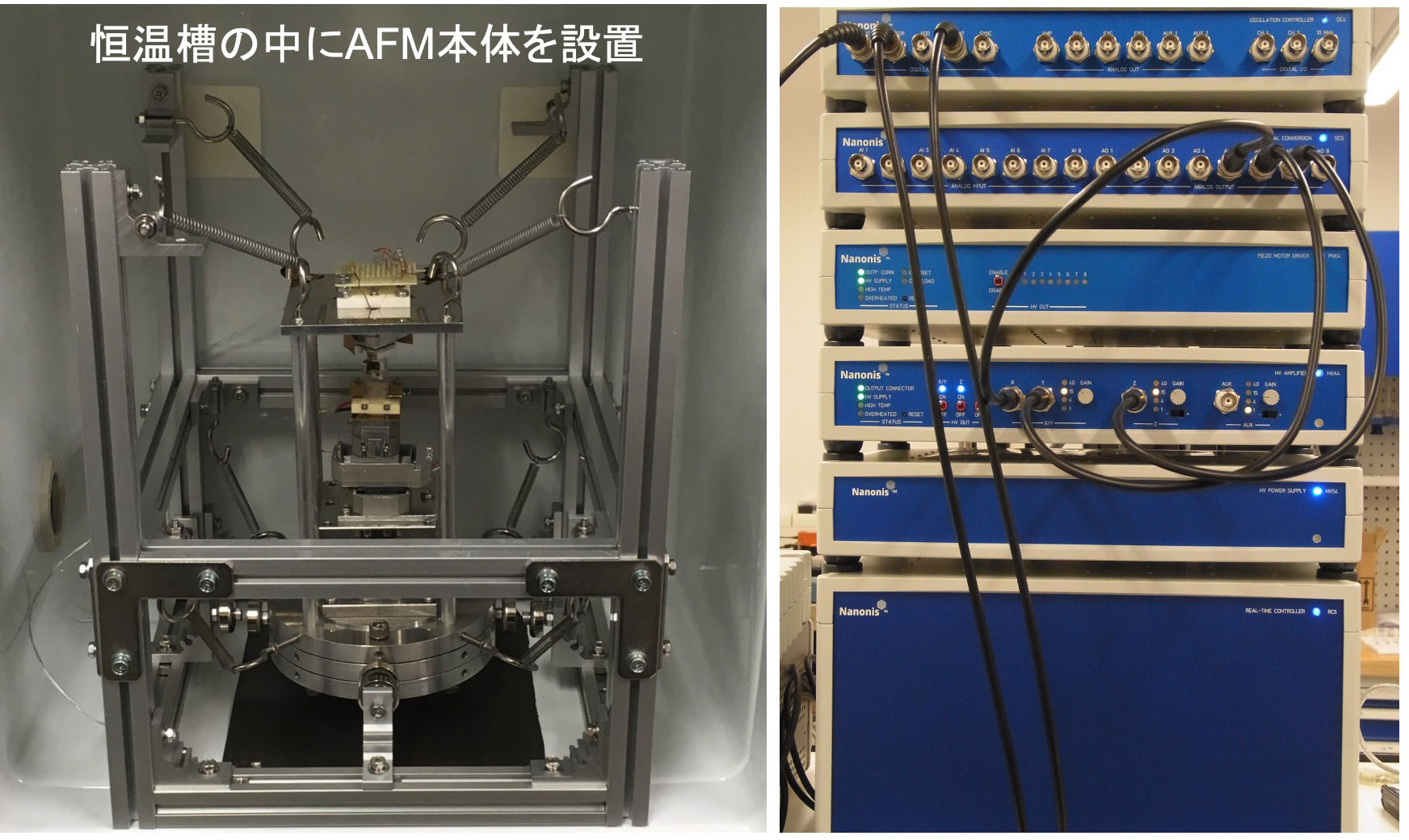
大気中駆動FM-AFM。FM-AFM用の力センサーには、独自開発の共振再調整(RTF)力センサーを用いている。
自然科学5号館 106号室
Research Topics
We have developed Frequency Modulation Atomic Force Microscopy (FM-AFM) and Scanning Tunneling Microscopy (STM). FM-AFM is also called non-contact Atomic Force Microscopy (nc-AFM) because it detects the weak attractive force between tip and sample, and they are not in contact when it is used in an ultra-high vacuum. In our research papers, it is referred to as UHV nc-AFM and FM-AFM in ambient condition. In this website, it is referred to as FM-AFM.
Atomic Force Spectroscopy
Toward atom-resolution nanomechanics we often measure the shift of resonance frequency (∆f) of a force sensor used in an atomic force microscope (AFM) using a frequency-modulation (FM) technique; we call this method FM-AFM. The value of ∆f negatively increases with decreasing AFM tip–sample separation when the attractive forces act between the tip and the sample. When the bias voltage (V) between them is changed while the tip–sample separation is kept constant, –∆f behaves proportionally to V2 in the region of dominant electrostatic interactions. In general, at the wide separations where only van der Waals force and the electrostatic force act as long-range forces, –∆f changes along with the separation and the bias voltage; the surface plot in the figure below shows such changes of –∆f. Now then, how does the surface plot emerge at the closer separations in the figure where chemical bonding forces act as the short-range forces?
At the dawn of establishing quantum mechanics, Linus Pauling described in his great book of “The Nature of the Chemical Bond (the first edition published in 1939)” that the chemical bond is explained as the quantum mechanical resonance between the outermost electronic states of two atoms in proximity, the energy levels of which are so close. This means that if the energies of the two isolated atoms are not so matched, the chemical bond between the two atoms is not produced.
We discovered that strong attractive forces acted between the specific atoms on a sample surface and the AFM tip in close proximity, when a certain specific voltage is applied between the tip and the sample. This phenomenon seemed to correspond to the quantum mechanical resonance between the surface atom and the tip atom under the conditions that the energy levels of the atoms are in agreement; this could be the chemical bond. Then, using our custom-made UHV FM-AFM/STM_3, in which we were able to measure the tunneling current passing between them, we conducted the force spectroscopy while the tip was being scanned over the surface and instantly the force–bias voltage curves were measured at a constant tip–sample separation. We measured the ∆f–bias voltage curves while the tip–sample separation was decreased stepwise over the surface Si atom. As shown in the figure below, we found the sharp peaks at the specific bias voltages, and the peaks increased with decreasing separation. This indicated that the chemical forces could be produced by tuning the bias voltage between the AFM tip apex atom and the sample surface atom, corresponding to the quantum mechanical resonance, which is the concept introduced by Pauling.
Our experimental finding implied that we could extend the concept of the chemical bonding between two isolated atoms to the surface chemical bonding of two pieces of condensed matter by tuning the bias voltage between them. Our experimental sample was a Si surface and a Si tip with covalently bonding. We are studying the resonating forces between heterogenous atoms in condensed matter by use of our developed force spectroscopic method, and further extending this method of bias force spectroscopy to fabricate nanoscale structures.
Evaluation of surface resistances with Joule heat dissipation energy
In the FM-AFM to measure the forces between the tip and the sample, we measure the shift of resonance frequency ∆f of the force sensor of a tiny cantilever having an atomically sharpened tip while the cantilever is being oscillated at a constant amplitude; the ∆f roughly corresponds to the distance derivative of the force acting between the tip and the sample. Meanwhile, when the mechanical energy stored in the oscillating cantilever dissipates through nonconservative interactions, the oscillating amplitude becomes smaller. Then, the sinusoidal signal to excite the cantilever oscillation at a constant amplitude becomes larger to compensate the decrease in the amplitude; we use the feedback control to do so. Therefore, by measuring the change in the excitation sinusoidal signal, we can evaluate the dissipative energy through the nonconservative interactions. It is noted that we can simultaneously measure the tunneling current passing between the tip and the sample by applying a bias voltage between them.
When the tip and the sample are conductive, and a bias voltage VS is applied, ∆f can be decomposed into ∆fvdW, ∆fele, and ∆fSR that are caused by the van der Waals force, the electrostatic force, and the short-range forces, respectively, as follows:
![]() (1)
(1)
Meanwhile, the dissipation energy D can be decomposed into Dint, DJoule, and DSR that are caused by the internal friction of the cantilever, the displacement current passing the resistance in the electric circuit involving the tip and the sample, resulting in Joule heat, and the nonconservative short-range interactions between the tip and the sample in close proximity, respectively, as follows:
![]() (2)
(2)
Now we focus on ∆fele and DJoule at wide separations where the short-range forces can be ignored. Here, we define the contact potential difference VCPD of the sample with respect to the potential of the tip. When the resistance in the circuit can be represented by resistance RJ, the relationship between ∆fele and DJoule can be expressed as follows:
(3)
(4)
where f0, A, and k are the resonance frequency of the cantilever at free, its oscillation amplitude, and spring constant, respectively; VS is the sample bias voltage, rtip is the tip radius, and d is the closest tip–sample separation during the cantilever oscillating. Comparing eq. (3) with eq. (4), it is appreciable that both ∆fele and DJoule are proportional to d–1/2 and (VS–VCPD)2. By dividing eq. (4) by eq. (3), the equation below is obtained:
(5)
From eq. 5, it is apparent that ∆fele is proportional to DJoule independently of the distance and bias voltage. The proportional coefficient contains RJ, and the other parameters are estimated from other measurements. Thus, by simultaneous measurements of ∆fele and DJoule, we can evaluate RJ from the proportional coefficient between them.
For a sample of Si(111)-(7×7) and a Si tip, we measured ∆fele and DJoule at a separation of a few nm under sweeping bias voltage, as shown in the figures below.
From the plots in the figures, we made the plots of DJoule as a function of ∆fele in the following figure. The plots show the linear relationship we anticipated, clearly indicating the proportional relationship between ∆fele and DJoule. From the proportional coefficient, it is possible to evaluate the resistance RJ in the region where the displacement current passed.
Here, we discuss on which resistance in the circuit was measured. We compared the values obtained when we externally inserted a resistor in-series in the circuit and also deposited a thin film on the sample surface to change the surface resistance. As a consequence, we reached a conclusion that we measured the resistance around the tip apex and the sample region underneath its surface with a depth of the tip radius. We expect that this measurement of dissipation energy can infer the surface resistance of sample in the region of a few tens nm depth in noncontact.
Energy dissipation unveils atomic displacement
Since the advent of STM in 1981, the reconstructed surface of Si(111)-(7×7) was successfully observed with atomic resolution by many researchers using STM and FM-AFM. In the STM and FM-AFM images, the individual Si adatoms on the surface were observed. The atomic arrangement of Si(111)-(7×7) was incontrovertibly explained by dimer-adatom-stacking fault (DAS) model.
In the past, the increase in dissipation energy over the adatom was reported, corresponding to pulling up of the adatom through the nonconservative interaction with the AFM tip. Our finding dissipation energy over the hollow sites was about 0.2 eV/cycle, that is, 0.2 eV per one cycle of the cantilever oscillation. This value was in agreement to the difference in Si coordination energy between the adatom site and the hollow site, which is the most stable and the meta stable site, respectively. We further conducted the experiment using a partially hydrogen (H)-terminated surface of Si(111)-(7×7). Therein, the dangling bonds of the adatoms and the rest atoms were partially terminated with H atom, leading to loss of reactivity of the dangling bond. As a result, we confirmed that, when both adatom and its neighboring rest atom were not terminated with H, the dissipation energy increased at the middle site between the adatom and the rest atom, that is the hollow site. We discussed the mechanism as follows: when the Si tip atom was brought closer to the hollow site, the bonding between the Si tip atom and the Si adatom was formed, and partly broke the back bond of the Si adtom to the surface. Further tip approach on the cantilever oscillation moves the Si adatom toward the hollow site, as if the tip flips the tetrahedron of Si atoms on the surface, and stabilized the Si adatom over the hollow site. Next, on the tip retraction, the bond between the Si tip atom and the adatom was broken. Afterward, the adatom at the hollow site returned to the original adatom site with the most stable coordination. At the moment the extra bonding energy is released, corresponding to the difference in the coordination energy between the hollow site and the adatom site. This atomic motion seemed to be repeated by the tip approach and retraction on its oscillation. The force–distance curve would have hysteresis because the bonding configuration around the Si adatom was altered between the approach and the retraction on the cantilever oscillation. The attractive force on the tip retraction would be stronger than that on the tip approach, because the adatom at the hollow site is located just under the Si tip. The area of the hysteresis in the force–distance curve should be equal to the dissipation energy as a mechanical work, which we measured. At present, for confirmation, we are simulating the atomistic motion on the basis of the first-principle calculations to evaluate the dissipation energy during one cycle of the tip oscillation.
nanometer-thick water film
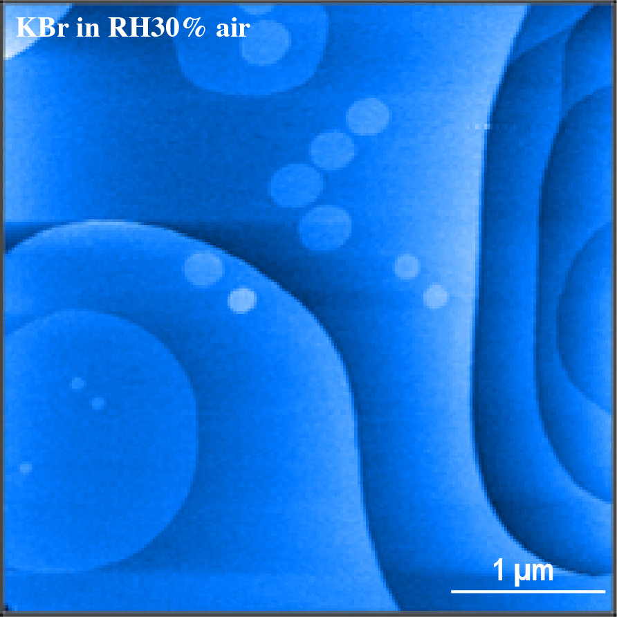
On hydrophilic solid surfaces, water is adsorbed, whose thickness depends on the humidity of the environment. For example, at a low humidity, one layer of water molecules is adsorbed on the surface of a cubic crystal of salt (NaCl) that looks smoothly trickled. This layer has no ability of dissolving the salt, differently from bulk water. Meanwhile, in a salt-saturated water solution, at the interface between the remained salt crystals and the solution, water molecules form a hydration layer with Na+ and Cl– ions on the crystals. Besides ionic crystals, the hydration layer is formed on a hydrophilic solid surface. In a simplified picture to represent the hydration layer, the water molecules are depicted to form a stable structure without mobility. But, in fact, the lifetime of being in a stable hydrated structure is short; the water molecules in bulk water are very often exchanged with the water molecules hydrated on the surface.
What happens at the interface between the bulk water and the solid surface under high humidities, where the water adsorbed layer has about 10-molecule thickness, i.e. a few nanometers thickness? We, our nano physics lab, revealed that the water layer exhibits quasi-stabilized mechanical properties; the mobility of water molecules in the layer is lower and the mechanical properties of the water molecules are between liquid and solid, similar to ice structures. Thus, we are exploring the thin water layers on the solid surfaces; we name them nanometer-thick water films.


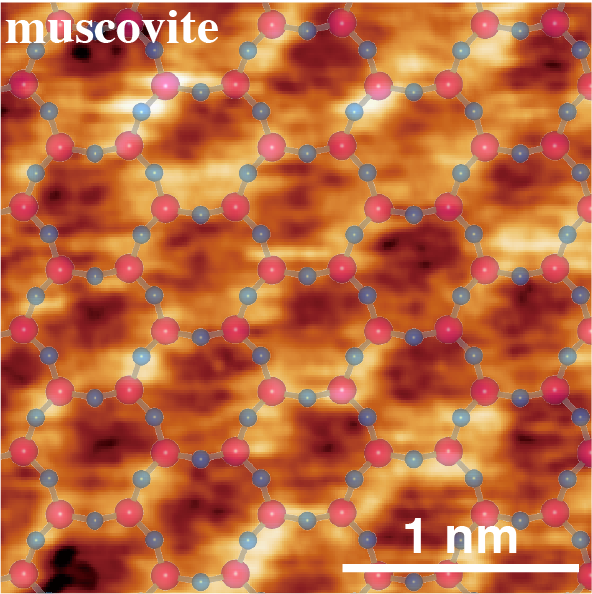
Nanometer-thick water film on mica
Mica is a group name among various silicate minerals; some kinds of minerals with slightly different components and crystal structures belong to this group. In the mica group, muscovite (KAl2(Si3Al)O10(OH)2) has been frequently used as a substrate for AFM observation. Mica is layered materials that are easily cleaved with Scotch tape; the cleaved surface exhibits atomically flat. So, it is useful to prepare biomolecule samples for AFM. We investigated the hydration structure of the nanometer-thick water films grown on muscovite at high humidities. At 25 °C in lab environment, we found the structural defects of the hydration that look meta-stable on the muscovite surface. In general, bulk water has no stable defects, differently from solid state. This indicates that the nanometer-thick water film has unique properties as quasi-stabilized matter, which holds a value of a new phase of materials to be analyzed and exploited.
The structure of muscovite
The muscovite has a K+ layer between tetrahedron sheets of SiO2. Cleavage along the layer randomly leaves the half of K+ ions of the layer on the cleaved surface, because the other half of K+ ions are located on the counter surface of cleavage. The Si atoms of the tetrahedron sheet are replaced by Al atoms at a rate of 1/4. Consequently, the tetrahedron sheet has negative charge, which is compensated with the positive charge of K+ ions; the charge neutrality is kept as a whole.
Hydration structure of the interface between the nanometer-thick water film and the muscovite surface
We observed the periodic patterns in the FM-AFM images at tip heights below 1 nm from the muscovite surface; the fundamental periodicities of the patterns are in agreement to the atomistic structure of muscovite surface. It is noticeable that the periodic patterns slightly changed with decreasing tip height. The right figure, at the furthest height among the images shown here, corresponds to the third hydration layer. By approaching the tip closer to the surface, the second and the first hydration layers and the water adsorbed layer were consecutively observed, as shown in the figures. To clearly see the structures, we superimposed the atomic lattice pattern of muscovite on the figures. In the FM-AFM images of the muscovite surface in bulk water, the similar patterns were reported for the first and second hydration layers. However, the periodic structure of the third hydration layer was not observed in bulk water. This implied that the bonding between the nanometer-thick water film and the muscovite surface is stronger than that in bulk water, and their bonding length are shorter. In the left image for the adsorbed layer, green circle symbols are marked over the bright dots, where the K+ ions are probably left and located over the cavities on the muscovite surface. Over the cavities besides the marked ones, water molecules seems to be adsorbed, resulted in weak bright dots in the image. This recognition of the K+ left over the cavities was first demonstrated in this study.
Defect structure of the nanometer-thick water film
By repeating the observation of the first and second hydration layers, we sometimes observed some defective structural patterns in the hydration layers. We speculated that the muscovite surface under the observed defective positions had defects. In the hydration layer, water molecules are connected each other via hydrogen bonding. Thus, if the mobility of water molecules in the film was enough high, it was not likely that the defect structures remained for a certain long period in this experiment, for the thickness of 2 nm, i.e., ten-molecule thickness. It is suggested that the structure of the film is similar to that seen in Frank-van der Merwe (FM) growth mode, which is often employed to explain the mechanism of a layer-by-layer epitaxial film growth in solid. When the substrate has a defect, the layer-by-layer growth in FM mode would be disturbed around the defect. In the nanometer-thick water films, we have a chance to find the substrate defects through the quasi-stabilized hydrated structure. Meanwhile, for solid state films, if the AFM tip breaks the structure of the film surfaces, its defective traces would be observed over a long period. However, in the nanometer-thick water films, if the AFM tip breaks the structure of the film, the induced defective structure would disappear quickly after the tip is retracted. For instance, we have repeatedly observed the regular periodic patterns depending on individual hydration layers. This reflects the flexibility of hydrogen bonding. For the water molecules farther from the substrate, though their bonding seems gradually weaker, their mobility is still lower than that in bulk water. It is also pointed out that the ordering structure formed at the interface between the air and the water can constrain the mobility of the water molecules at the interface. Importantly, since the nanometer-thick water film is intensely restricted between the substrate and the air, the unique mechanical properties of the film come out, differently from those of bulk water.
ReTuned Fork (RTF) force sensor
For a force sensor in FM-AFM, commercial Si cantilevers have been often used, which are oscillated at their resonance frequency. For the FM-AFM operated in air, we have also used them. On the other hand, to detect the frequency shift ∆f at a very small amplitude with a high sensitivity, we developed a retuned tuning fork (RTF) sensor from a quartz tuning fork for a watch.
To improve the force sensitivity for the FM-AFM, a high Q-value of the force sensor is indispensable; high Q-value means low loss mechanical energy on the oscillation. In the tuning fork, its two prongs have the same resonance frequency, which have been tuned in the fabrication process. The high Q-value is achieved in anti-phase oscillation mode of the two prongs. For the FM-AFM, we have to attach a tip on the one prong, resulted in deterioration of the Q-value due to their unmatched resonance frequencies between the two prongs. Thus, we cut a tiny part at the end of the one prong, where the tip is attached. The mass of the part is almost equal to the mass of the tip and the adhesive. This can provide the same resonance frequency of the two prongs. In our hand-made process, we fabricated the RTF sensor, in which the resonance frequency was retuned with a high Q-value.
Fabrication procedure of RTF sensor
The prong size of the quartz tuning fork is 2×0.2×0.1 mm. We ground a tiny part of the end of prong. Afterward, we attach a sharpened tip of 0.1 mm in length to there. These processes are done by our hands under the stereo optical microscope.
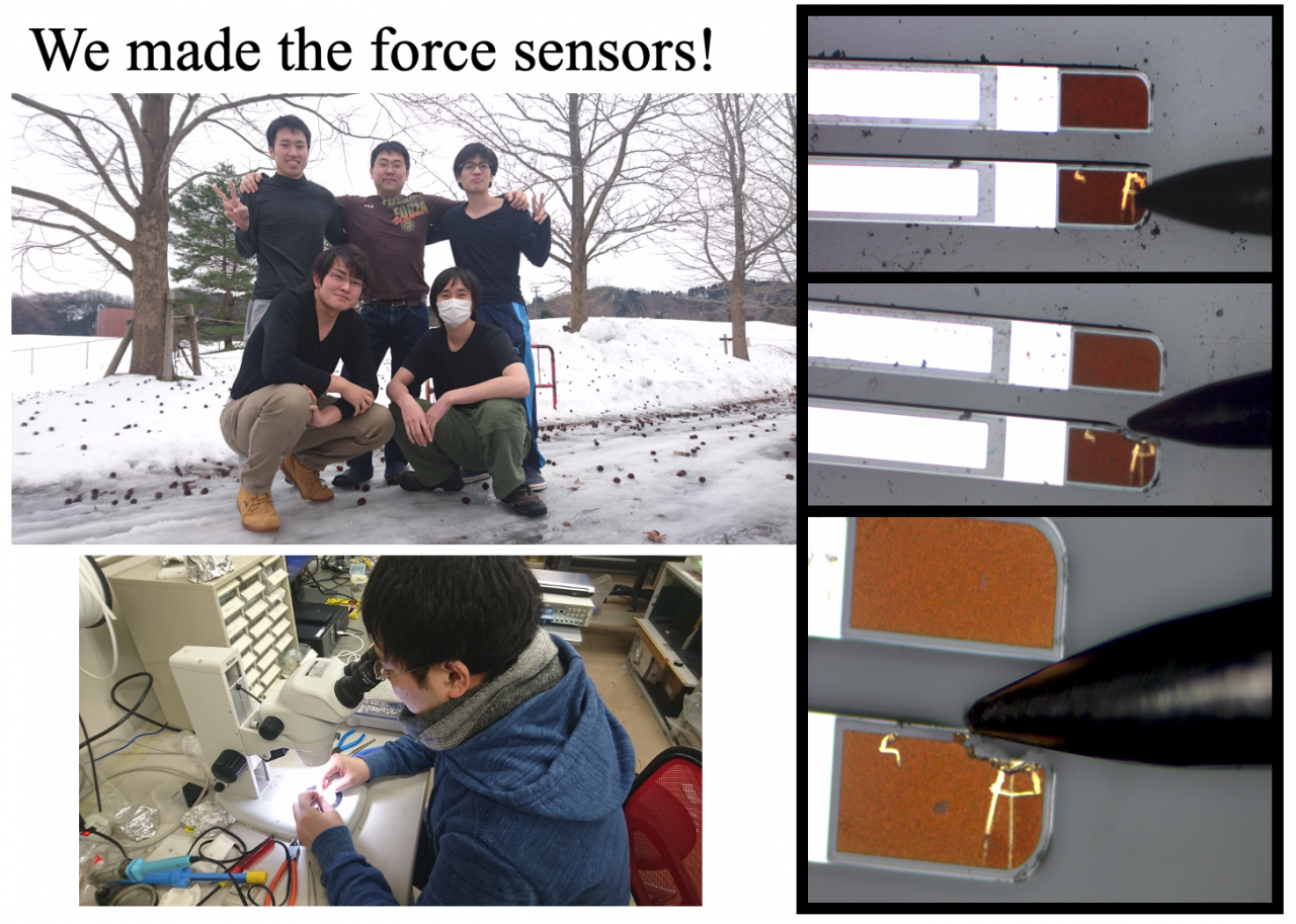
Image Gallery
Developed Instruments
UHV LT FM-AFM/STM_1
UHV LT FM-AFM/STM with retuned fork (RTF) force sensor 1
This FM-AFM/STM equipped with a liquid helium tank cryostat. A retuned fork (RTF) force sensor is used.
At Room 103-2 in Natural Science and Technology Hall 5.
UHV FM-AFM/STM_2
UHV FM-AFM/STM with retuned fork (RTF) force sensor 2
A retuned fork (RTF) force sensor with a W tip is used. The W tip is sharped by flame etching.
At Room 103-1 in Natural Science and Technology Hall 5.
UHV FM-AFM/STM_3
UHV FM-AFM/STM with piezoresistive Si cantilever
This FM-AFM/STM was first build up by Prof. Arai. It has a fluorescent screen for FIM/FEM in the UHV chamber. FIM/FEM images of tips can be obtained.
It is placed at the collaborator’s Lab in Japan Advanced Institute of Science and Technology (JAIST).
ambient FM-AFM_4
ambient FM-AFM 4
This FM-AFM system was developed with the support by the SENTAN Program of the Japan Science and Technology Agency.
At Room 410-411 in Natural Science and Technology Hall 5.
ambient FM-AFM_5
ambient FM-AFM 5
The FM-AFM head was installed in a thermostatic chamber. A retuned fork (RTF) force sensor is used.
At Room 106 in Natural Science and Technology Hall 5.